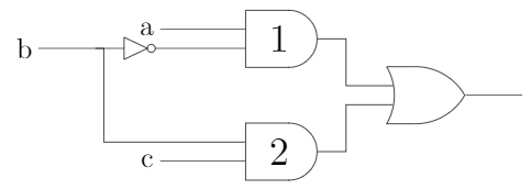
In the diagram above, the inverter (NOT gate) and the AND-gates labeled $1$ and $2$ have delays of $9, 10$ and $12$ nanoseconds (ns), respectively. Wire delays are negligible. For certain values $a$ and $c$, together with certain transition of $b$, a glitch (spurious output) is generated for a short time, after which the output assumes its correct value. The duration of glitch is:
- $7\;\text{ns}$
- $9\;\text{ns}$
- $11\;\text{ns}$
- $13\;\text{ns}$