
Let us plot the logic states at the various points of interests in this circuit.
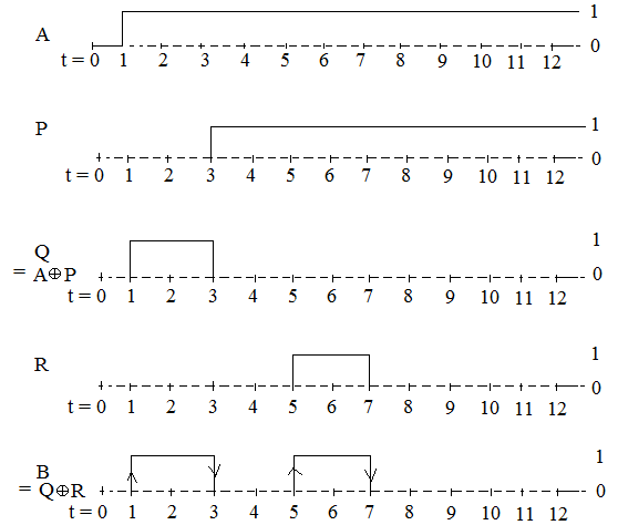
$\underline{\text{Explanation}:}$
Note that,  is not an inverter but a buffer used for introducing delay.
∴ Output at 'P' and 'R' will be obtained at $2$ ns and $4$ ns respectively after the change in their inputs.
Hence, waveforms of 'P' and 'R' are shifted by $2$ ns and $4$ ns as compared to their inputs.
Also, note that 'Q' and 'B' are plotted using their corresponding input waveforms.
Finally, we can see that there are $4$ changes in logic levels in the waveforms of 'B'.
Answer is : Option D