Here, input “0” is considered as $I_0$ and input “1” is considered as $I_1$ and output Q is considered as Y for the given MUX.
As we can see in the given figure that $I_0 = Y,$ $I_0$ is storing the previous state of output $Y.$
Now, the basic function of $D$ Latch is:
$1)$ When Enable(E) = $0,$ Output state has the same its previous state, we call it as Memory State or you can say informally as $Q_{n+1} = Q_n$
$2)$ When Enable(E) = $1,$ Output variable = Input variable
Now, here, make the setting as:
Input: $I_1$ and Enable(E)= $S$
Now, As we have already seen that $I_0$ is storing the previous state of output. So, Say, previous state of output is $Y_{old}$ and Next state of output is $Y_{new}$
Now, According to the equation of $2 \times 1$ MUX i.e. $Y= \overline{S}I_0 + S I_1$
Since, $I_0 =Y_{old}$
Hence, we have
$Y_{new} = \overline{S}Y_{old} + S I_1$
Now,
$1)$ Make Enable(E)= $S = 0$, we get,
$Y_{new} = Y_{old}$ (i.e. Memory State for the D Latch)
$2)$ Make Enable(E)= $S = 1$, we get,
$Y_{new} = I_1 $ (i.e. output = input)
Hence, given circuit is equivalent to $D$ Latch.
Therefore, $\textbf{(B)}$
Edit:
There is a misconception that "In latches, clock is not present". The following points are addressing this misconception.
(1) Latches and flip flops are the “bistable” elements because it is having two "stable" states Q=0 and Q=1 (stable means they are consistent with the original assumption on output Q).
(2) It should also be noted that a circuit can also have a third possible state with both outputs which is approximately halfway between 0 and 1 and this is called a metastable state.
(3) Since latches and flip flops are bistable stable element and so they are having $\log_2 2$=1 bit of information. Using the past values of output Q we can explain the future values of output Q and these bistable elements are also having the controlled inputs like S and R in S-R Latch or D in D-latch that control the states of output Q.
(4) In D-Latch, "D" stands for the "data" and it is a controlled input which control the next state of output Q.
(5) The clock input "CLK" decides when the input state should be changes.
Please find the attachment from the book “digital design and computer architecture by harris & harris”:
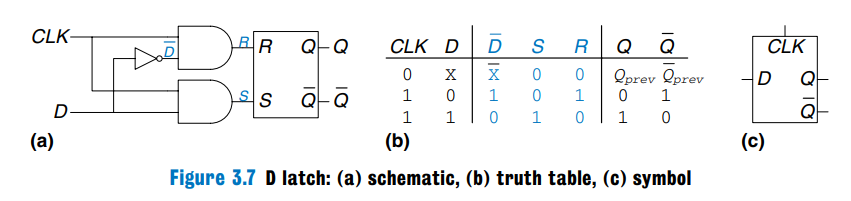
here we have used the clock input "CLK" but it is still a D-Latch.
(6) Now, comes to the D flip-flop,
A D- flip flop can also be implemented by two D-latches as can be seen below and it is also from the same book as above:

(7) Flip flop works on the rising or falling edge (clock edge) of the clock so, the correct statements are "latch is level triggered" and "flip flop is edge triggered".
How we can implement the edge triggering, you can refer the above book for more details and all the above points are taken from the same book.
The triangle in the symbols denotes an edge-triggered clock input and here in the question, we are not implementing the "edge clock", "S" is a just simply a select input for the conventional multiplexer.

