Consider the following circuit. $A = a_2a_1a_0$ and $B=b_2b_1b_0$ are three bit binary numbers input to the circuit. The output is $Z=z_3z_2z_1z_0$. R0, R1 and R2 are registers with loading clock shown. The registers are loaded with their input data with the falling edge of a clock pulse (signal CLOCK shown) and appears as shown. The bits of input number A, B and the full adders are as shown in the circuit. Assume Clock period is greater than the settling time of all circuits.
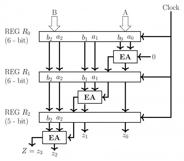
a. For 8 clock pulses on the CLOCK terminal and the inputs $A, B$ as shown, obtain the output $Z$ (sequence of $4-bit$ values of $Z).$ Assume initial contents of $R_0, R_1$ and $R_2$ as all zeros. $$\begin{array}{|l|l|l|l|l|l|l|l|l|} \hline \text{A} & 110 & 011 & 111 & 101 & 000 & 000 & 000 & 000\\\hline \text{B} & 101 & 101 & 011 & 110 & 000 & 000 & 000 & 000 \\\hline \text{Clock No} & 1 & 2 & 3 &4 &5 &6 &7&8\\\hline \end{array}$$
b. What does the circuit implement?