55,380 views
122 122 votes

A 4-bit carry look ahead adder, which adds two 4-bit numbers, is designed using AND, OR, NOT, NAND, NOR gates only. Assuming that all the inputs are available in both complemented and uncomplemented forms and the delay of each gate is one time unit, what is the overall propagation delay of the adder? Assume that the carry network has been implemented using two-level AND-OR logic.

  1. 4 time units
  2. 6 time units
  3. 10 time units
  4. 12 time units

23 Answers

0 0 votes
the only thing we have to notice here is that FAN IN is not given in question ,so we can take as we want. and then all the carry will be generated in equal amount of delay(C0,C1,C2,C3). therefore maximum delay will be because of S3 that is last sum ,s3=p3xor c3.
0 0 votes

If nothing is mentioned take fan-in for a logic gate = 2 inputs and they will say in the question whether to take half adder or full adder for the 1st stage of LSB addition(ripple carry adder).

Propagation delay In carry look-ahead adder(n bit adder):-

Carry look-ahead adder works in three phases:-

In carry look-ahead adder all Pi, Gi terms are computed simultaneously after that all carry terms are computed simultaneously and after that all sum terms are computed simultaneously.
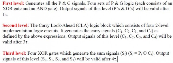
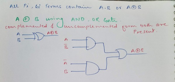
The first level will take 2 time unit to generate all Pi, Gi terms using AND-OR gate in 2 levels only if variables are given in both complemented and uncomplemented form.
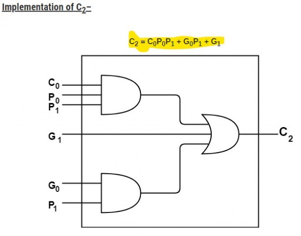
similarly 2nd level will also take further 2 time unit for generating the all carry terms.
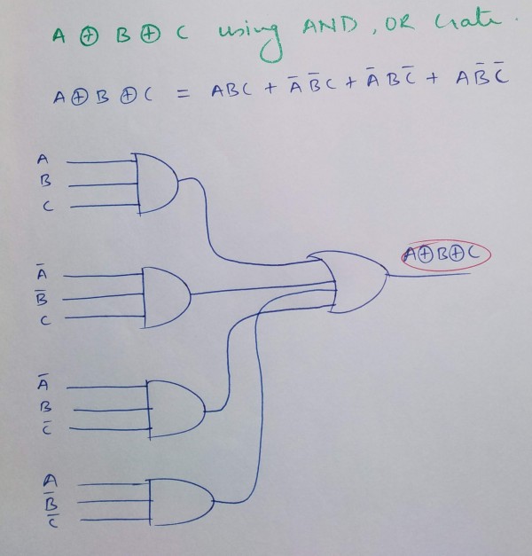
and after that to produce the sum terms it will take further 2 time unit. so total propagation delay is 6 time unit.
Note:- Any simple or complex logical function can be written in SUM OF PRODUCT form and can be realized using 2-levels of AND, OR gate only if both complemented and uncomplemented forms are given.


Now lets extend this question further for Ripple carry adder:-

In ripple carry adder(n bit adder):-              Assume Full adder is used for LSB computation, not half adder

Tpropagation =(n-1)* T.carry generation time by one full adder+ max(T.carry, T.sum)

                      = 3     *    2  (2 because C=AB+BC+AC can be implemented in 2 levels of AND, OR gate) + max(2, 4)

T.sum=4,       because A⊕B can be implemented using 2 levels of AND, OR gate only if variables are given in both complemented and uncomplemented form as mentioned above. then further one more XOR with C. so total 4 level of AND, OR gate.

Tpropagation for ripple carry adder = 10

for more-https://www.gatevidyalay.com/delay-in-ripple-carry-adder/

edited by
0 0 votes

>Though my this solution is same as given by ryan sir, but I have shown the stages in diagram for simple visualization purpose. Main thing to notice is , we have to implement every function by using 2- levels AND/OR realization (In SOP form), even as per question we can not use xor gate.)

0 0 votes

Answer - (A) 4 units


Two level logic means that the logic design uses maximum two logic gates between input and output. This does not mean that the fan in of the logic gates is 2.

[Also it does not imply that the whole design will contain only two logic gates.It just means that a single path from input to output may contain no more than two logic gates.For two-level logic implementation, we consider four logic gates i.e. AND GateOR GateNAND Gate, and NOR Gate.

Ref: https://www.electricaltechnology.org/2018/05/two-level-logic-implementation-combinational-logic-implementation.html]

Hence, the total time to generate carry will be the delay due to only two logic gates i.e. 2 units.

After knowing the value of each carry, each sum bit can be calculated parallely in 2 time unit delays. 

Thus, the total delay will be 4 units.

In case you are still confused, let us understand this in more detail.

In general we consider the fan-in of AND and OR gates to be a and b respectively and then calculate the carry delay as 

T1 = (levels of AND gates)*(time delay of each AND gate) + (levels of OR gates)*(time delay of each OR gate)

      = ceil(loga(n+1))*(Tand) + ceil(logb(n+1))*(Tor)

However, here it is already given that we are using two level AND-OR logic. 

So, ceil(loga(n+1)) = 1 and ceil(logb(n+1)) = 1   .....eq(1)

and, T1 = 1*1 + 1*1 = 2 time units.

From eq (1), we can say that a >=n+1 and b>=n+1. So we can even implement the sum circuit in two levels. The time delay for sum circuit will also be T2 = 2 units

The total delay will be T = T1 + T2 = 4 units

Answer:
Position:
Show:

Related questions

55 55 votes
5 answers 5 answers
27.1k
27.1k views
Kathleen asked Sep 18, 2014
27,086 views
Consider the partial implementation of a $2-bit$ counter using $T$ flip-flops following the sequence $0-2-3-1-0,$ as shown below.To complete the circuit, the input $X$ sh...
39 39 votes
4 answers 4 answers
12.1k
12.1k views
Kathleen asked Sep 18, 2014
12,077 views
Consider a multiplexer with $X$ and $Y$ as data inputs and $Z$ the as the control input. $Z=0$ selects input $X$, and $Z=1$ selects input $Y$. What are the connections re...
44 44 votes
2 answers 2 answers
16.3k
16.3k views
Kathleen asked Sep 18, 2014
16,299 views
Which are the essential prime implicants of the following Boolean function?$f(a, b, c)= a' c+ ac'+b' c$$a' c$ and $ac'$$a' c$ and $b' c$$a' c$ only.$ac'$ and $bc'$
46 46 votes
5 answers 5 answers
19.4k
19.4k views
Kathleen asked Sep 18, 2014
19,356 views
A circuit outputs a digit in the form of $4$ bits. $0$ is represented by $0000, 1$ by $0001, \ldots, 9$ by $1001$. A combinational circuit is to be designed which takes t...