The circuit given can be designed as:

State table can now be generated as:
| Q0 |
Q1 |
Q0N |
Q1N |
| 0 |
0 |
0 |
0 |
| 0 |
1 |
1 |
1 |
| 1 |
0 |
0 |
1 |
| 1 |
1 |
1 |
0 |
Now, transition diagram is:
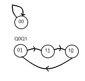
Since, the output is tapped at Q1, So, output will be (including the initial state '0' at D- FF): 0110110....
Correct Answer: (A).