retagged by
80 views
2 votes
2 votes

In the circuit shown below, $\mathrm{P}$ and $\mathrm{Q}$ are the inputs. The logical function realized by the circuit shown below is

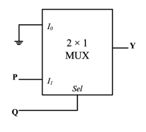
  1. $\mathrm{Y}=\mathrm{PQ}$
  2. $\mathrm{Y}=\mathrm{P}+\mathrm{Q}$
  3. $\mathrm{Y}=\overline{\mathrm{PQ}}$
  4. $\mathrm{Y}=\overline{\mathrm{P}+\mathrm{Q}}$
retagged by

1 Answer

Answer:

Related questions

152
views
2 answers
3 votes
GO Classes asked Oct 12, 2023
152 views
The logic function implemented by the circuit below is (ground implies a logic $\text{“0”})$\text{F=AND(P,Q})$\text{F=OR(P,Q})$\text{F=XNOR(P,Q})$\text{F=XOR(P,Q})$
128
views
1 answers
4 votes
GO Classes asked Oct 12, 2023
128 views
The figure below shows a multiplexer where $S_{1}$ and $S_{0}$ are the select lines, $I_{0}$ to $I_{3}$ are the input data lines, $\text{EN}$ is the enable line, ... {Q}R.$PQ+Q\overline{R}.$P\overline{Q}R+\overline{P}Q.$\overline{Q}+PR.$
107
views
2 answers
2 votes
GO Classes asked Oct 12, 2023
107 views
An $8$- to $1$ multiplexer is used to implement a logical function $Y$ as shown in the figure. The output $Y$ ... D$Y= \overline{A} \: \overline{B} \: D + A \: \overline{B} \: C$
98
views
2 answers
2 votes
GO Classes asked Oct 12, 2023
98 views
Consider the $ \text{2-bit}$ multiplexer $\text{(MUX)}$ shown in the figure. For $\text{OUTPUT}$ to be the $\text{XOR}$ of $\text{C}$ and $\text{D},$ ... , A_{3} = 0$A_{0} = 1, A_{1} = 1, A_{2} = 0, A_{3} = 0$